Printed hybrid electronics and aerosol jet printing
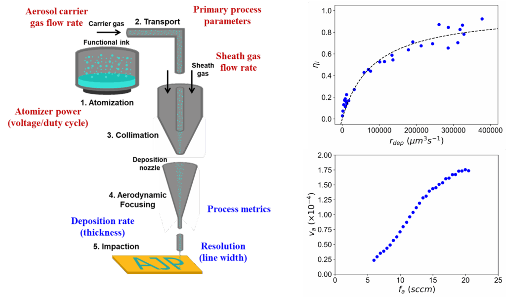
Our research is focused on additive manufacturing technologies for electronic materials. We specifically focus on a digital printing method called aerosol jet printing, which deposits micron-scale droplets of functional liquid inks to produce fine (~20-50 micron) patterns. This can be used to fabricate electronic devices (e.g., sensors, antennas), print wiring to manufacture more complex circuits include conventional microelectronics and passive electronic devices, and target more advanced structures including high aspect ratio pattern and composition gradients. Our work in aerosol jet printing (AJP) spans efforts to understand the physics of the printing process, and thus more rationally approach ink formulation and modification of the printing system; improve manufacturing reliability through unique process monitoring and control technologies; fabricate electronics on curved 3D surfaces by exploiting the high nozzle-surface offset during printing and digital motion planning; and develop new materials, including gradient patterning with multiple materials. Additional details related to each of these four core topics is included below.
Aerosol jet printing process fundamentals
We aim to establish a holistic framework to understand the physics of AJP, which can provide guidance for material development, process parameter optimization, and printing system design. This provides a versatile foundation for other research efforts, and is based on tailored experiments, computational modeling, and theory-driven analysis.